A stress test for copper-tungsten nanomultilayers
By Nicola Nosengo/NCCR MARVEL
Nanomultilayers are new materials with unique mechanical, optical and magnetic properties and high radiation tolerance. They are made by stacking alternating layers of two or more different materials – typically metals - on top of each other, in order to amplify and exploit the particular properties of their interfaces. They can be used for a wide range of applications including flexible electronics, microelectronics, batteries, optical coatings and more.
A key problem in predicting their behavior is understanding how stress can build up at their interfaces during manufacturing. Stress can be both compressive or tensile, and can cause delamination, when one layer is detached from the other or from the substrate, or degradation of the materials. But if controlled, the stress and the resulting deformation can also be exploited to fine-tune the material’s properties.
A new study just published in Acta Materialia combined theory, experiments and machine learning to model interface stress in a particularly interesting nanomultilayer, the one built with copper and tungsten. In doing so the authors, including scientists from Vladyslav Turlo’s group at Empa and Bill Curtin’s group at EPFL, managed to explain a perplexing anomaly spotted by experimentalists.
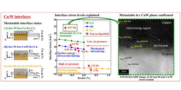
Simulated interfaces with varying structure and chemistry of interfacial layers (left) and their corresponding interface stresses with respect to in-plane strains (middle). Different interface states can be formed under different deposition conditions defined by Ar pressure, controlling the kinetic energy of incoming atoms. Modeling predicts that the extreme positive interface stress is caused by the formation of metastable bcc Cu-rich phase, which is confirmed by aberration-corrected high-resolution scanning transmission electron microscopy (right).
Claudia Cancellieri and her PhD student Giacomo Lorenzin - two experimentalists at Empa and also co-authors of the new publication - had previously noticed that, while depositing copper/tungsten multilayers on silicon, the substrate and film can curve due to stress. By measuring how laser beams are deflected by the curved material, they were able to track how stress evolves depending on the film’s thickness and the argon pressure used for deposition. They found a transition from negative to positive (or compressive-to-tensile) interface stress when thickness and pressure pass a certain threshold.
Turlo’s group set out to explain this transition. Standard Density Functional Theory could not do that, because it can only handle small systems, up to 1 nanometer per layer, while here the layer thickness was about 10 nanometers per layer. That left a huge discrepancy between DFT calculations and experiments.
A solution to this problem came from a neural network potential developed last year by Bill Curtin and his collaborator Manura Lyanage. This potential, developed through machine learning based on DFT calculations, dramatically improved the accuracy of calculation.
“Machine-learned potentials enabled large-scale simulations of many possible atomic-scale configurations with high chemical fidelity” says Curtin. “Even the nominal equilibrium interfaces between copper and tungsten are complex, and extending the study to examine possible non-equilibrium structures induced by the deposition conditions brought even more complexity. The Cu-W potential had to capture not only bulk and interface properties, but intermetallic, solubility, and other chemical features”.
Still, on the first attempt, even calculations with the new potential did not match experiments. “We checked factors like corrugation and interface roughness, but that was not enough to explain the discrepancy”, says Turlo. Some other factor had to be responsible for it. A few previous studies on other nanomultilayers, such as the silver/nickel and copper/vanadium ones, suggested that intermixing of the two materials at the surface could be the answer.
“We found no reports of the copper-tungsten interface chemistry from experimental studies”, says Yang Hu, a scientist in Turlo’s group and first author of the paper. “So we used atomistic simulations to model the different types of intermixing that can happen depending on the argon pressure”. At high argon pressure, she explains, there is low atom mobility and atoms will stay where they land. At low pressure there is higher atom mobility and intermixing is driven by the difference in surface energy of copper and tungsten. There is also ballistic intermixing, because tungsten is heavier than copper, and when it is deposited it knocks out atoms from the surface copper planes.
“In the end we introduced intermixed layers in the computation of interface stress by randomly replacing copper or tungsten atoms within the plane with the other type, aiming for a 50% mix, and we computed the interface stress" says Hu. "The results finally fitted the experimental data”. Moreover, the simulations predicted that extreme values of interface stress at low argon pressure must be the result of relatively thick intermixing layers at the interface.
The results were further validated by experimentalists, Claudia Cancellieri and Amit Sharma at Empa, who prepared and analyzed a new set of samples on rigid alumina substrates to minimize corrugation and roughness, showing that there is indeed a large interfacial intermixing similar to the one observed in copper/vanadium. “It is really difficult to show intermixing experimentally because of corrugation and roughness at the interface,” says Turlo. “You’re looking at a 50 nanometers slab and it’s hard to tell if you are seeing atomic intermixing or just a rough interface”. After annealing the samples, on the other hand, stress states come closer to what is predicted for a perfectly sharp interface.
“By proving that even a little intermixing can have such a huge effect, we show that manufacturers should pay attention to this aspect” says Turlo. And for Curtin, “this work validates our approach of using metallurgically-relevant atomistic configurations to train a bespoke potential for a specific alloy system, which was the enabling factor in a successful collaboration between theory and experiment”.
Reference
Yang Hu, Amit Sharma, Giacomo Lorenzin, Jeyun Yeom, Manura Liyanage, William A. Curtin, Lars P.H. Jeurgens, Jolanta Janczak-Rusch, Johann Michler, Claudia Cancellieri, Vladyslav Turlo, "Origin of interface stress enhancement and compressive-to-tensile stress transition in immiscible nanomultilayers" Acta Materialia, 297 (2025). https://doi.org/10.1016/j.actamat.2025.121323
Low-volume newsletters, targeted to the scientific and industrial communities.
Subscribe to our newsletter